


Never trust a computer you can’t throw out a window.
(Steve Wozniak)
Navigation

Kiwi - a 68k Homebrew Computer
September 7th 2012
Kiwi can be divided into several functional parts. Beside the CPU itself
a CPLD takes an central role in the overall functionality. It connects (glues) all
parts by serving their control lines.
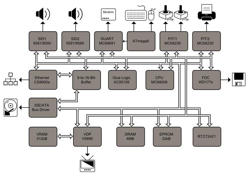
Hardware overview
Hardware overview
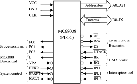
MC68008 - the central processing unit (CPU)
The MC68008, which has been used in the Sinclair QL, is the 8-bit variant
of the famous MC68000, that has been used in early Amigas, Macs and the Atari ST.
According to the reduced databus width, the MC68008 has to do twice bus accesses in comparison to the MC68000. Motorola states 60% speed average compared at the same clock. The MC68008 usually works in an asynchronous mode, which means bus accesses can be extended or shortened for slower or faster devices. The latter is done via the the low active DTACK signal; an accessed device pulls this line down to ground when the cycle is complete. In a read cycle, DTACK should be grounded when the data on the bus are stable. In a write cycle, DTACK should be grounded when the data on the bus is taken.
Motorola decided to give both, the MC68008 and the MC68000 a second, synchronous mode, which is supposed simplify the use of older MC6809 devices.
MC68008
Further signals include bus control for bus sharing with other bus masters (*BR and *BG) which is not used in Kiwi. There are three interrupt request inputs. These inputs represent the binary encoded interrupt level from 0 (no interrupt) to 7 (non maskerable interrupt, not used in Kiwi).
The following table illustrates all CPU vectors.
Exception vector table
According to the reduced databus width, the MC68008 has to do twice bus accesses in comparison to the MC68000. Motorola states 60% speed average compared at the same clock. The MC68008 usually works in an asynchronous mode, which means bus accesses can be extended or shortened for slower or faster devices. The latter is done via the the low active DTACK signal; an accessed device pulls this line down to ground when the cycle is complete. In a read cycle, DTACK should be grounded when the data on the bus are stable. In a write cycle, DTACK should be grounded when the data on the bus is taken.
Motorola decided to give both, the MC68008 and the MC68000 a second, synchronous mode, which is supposed simplify the use of older MC6809 devices.
MC68008
Further signals include bus control for bus sharing with other bus masters (*BR and *BG) which is not used in Kiwi. There are three interrupt request inputs. These inputs represent the binary encoded interrupt level from 0 (no interrupt) to 7 (non maskerable interrupt, not used in Kiwi).
The following table illustrates all CPU vectors.
| Vector number | Address | Function |
| 0 | 0x000 | Reset: Supervisor Stackpointer (SSP) |
| 1 | 0x004 | Reset: Program Counter (PC) |
| 2 | 0x008 | Bus Error |
| 3 | 0x00c | Address Error |
| 4 | 0x010 | Illegal Instruction |
| 5 | 0x014 | Null Division |
| 6 | 0x018 | CHK Instruction |
| 7 | 0x01c | Trapv Instruction |
| 8 | 0x020 | Privilege Violation |
| 9 | 0x024 | Trace |
| 10 | 0x028 | Line 1010 Emulator |
| 11 | 0x02c | Line 1111 Emulator |
| 12 | 0x030 | Reserved |
| 13 | 0x034 | Reserved |
| 14 | 0x038 | Reserved |
| 15 | 0x03c | Vector for non initialized Interrupts |
| 16-23 | 0x04c | Reserved |
| 24 | 0x060 | Spurious Interrupt |
| 25 | 0x064 | Level 1 Interrupt Autovector (V9990) |
| 26 | 0x068 | Level 2 Interrupt Autovector (IDE) |
| 27 | 0x06c | Level 3 Interrupt Autovector (CS8900a) |
| 28 | 0x070 | Level 4 Interrupt Autovector (WD177x) |
| 29 | 0x074 | Level 5 Interrupt Autovector (PI/T 2, Timer) |
| 30 | 0x078 | Level 6 Interrupt Autovector (DUART) |
| 31 | 0x07c | Level 7 Interrupt Autovector |
| 32-47 | 0x080 0x0bf | Vectors for TRAP Instruction |
| 48-63 | 0x0c0 0x0ff | Reserved |
| 64-255 | 0x100 0x3ff | User Interrupt Vectors |
Reset - what happens...
After power-on or a system reset, the CPU fetches the initial Program Counter
and the Supervisor Stackpointer. These vectors are addressed at 0x000000 and 0x000004. Therefore,
the CPU has to see ROM at these addresses. Unfortunately, it is very unpractical to have the whole
exception table in ROM, since this would prevent changing vectors. The trick is to count the first bus accesses and
overlay ROM just for the time the CPU needs to fetch both vectors. After fetching both vectors, the
CPU accesses RAM at 0x000000. This method is described in Motorola App. Note 897 "MC68008 Minimum
Configuration System".
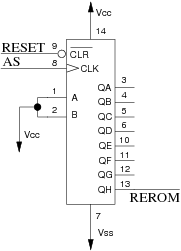
REROM generator
After Reset, all Qn-Outputs of the 74LS164 shift register are low, while the input is connected to a Pull-Up resistor. AS toggles with every single bus access. It takes eight (2*4 bytes) accesses to fetch both vectors. Every time AS goes low, the logic one is shifted one position. After eight accesses, the QH output changes from low to high. This signal (REROM) is used to overlay ROM at address 0x000000. This solution is transparent for the software.
Memory-map
As mentioned above, REROM is used to overlay ROM at address 0x000000. After
fetching PC and SSP, the system switches to its finally memory map:
Memory Map
The address decoding circuit is part of the CPLD XC95108.
| RAM | 0x000000 - 0x3dcfff |
| MC68681 Duart (RS-232) | 0x3ddxxx |
| V9990 Video Display Processor | 0x3dexxx |
| WD177x (FDC) | 0x3df7xx |
| SID 1 (left audio channel) | 0x3df8xx |
| SID 2 (right audio channel) | 0x3df9xx |
| MC68230 PI/T 1 (Joysticks) | 0x3dfaxx |
| MC68230 PI/T 2 (Parallel Port, Floppy) | 0x3dfbxx |
| RTC72421 Real Time Clock | 0x3dfcxx |
| IDE CS0 | 0x3dfdxx |
| IDE CS1 | 0x3dfexx |
| CS8900a | 0x3dffxx |
| ROM | 0x3e0000 - 0x3e7fff |
| RAM | 0x3e8000 - 0x3fffff |
Dynamic RAM
An 30 pin SIMM is used as main memory. These old DRAM modules have a
databus width of 8 bit. Dynamic RAM has a couple of advantages against static RAM.
It is smaller and cheaper than static RAM with the same capacity. The downside is that
it is slightly more complex to use dynamic RAM. First the address bus is multiplexed.
Meaning that one address line carries two address bit. DRAM chips have two control
signals to input either row address (RAS) or column address (CAS).

DRAM circuit
On the other hand, DRAM cells need to be refreshed frequently. A DRAM cell is built around an transistor and a capacitor and as every capacitor has some leakage, the cell would loose its stored information after some time. To circumvent this difficulty, the capacitor has to be recharged (refreshed) within a certain period. Thus, all cells within the accessed row are refreshed at once every time the DRAM is accessed. Since every cell has to be refreshed, it is not sufficient to rely on ordinary CPU accesses. There are numerous refreshing techniques, where Kiwi uses CAS before RAS refresh only. In a normal memory cycle (read or write) the order of strobing in the address is "RAS goes low before CAS goes low". If CAS is grounded before RAS, the DRAM performs an automatic refresh cycle. It keeps track of the last refreshed row and refreshes the next.
Refresh counter
MC68681 - RS-232, PS/2 Keyboard and Mouse
The MC68681 DUART has two serial interfaces. The first one is used
in conjunction with an MAX232 to form an RS-232 interface. It is available via an DB9 connector.
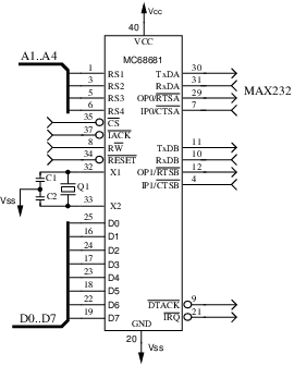
MC68681 (DUART)

MAX-232
The second serial interface of the DUART is directly connected to the ATmega8. The latter samples both PS/2 ports and sends data to the DUART.
PS/2 Interfaces
MC68681 (DUART)
MAX-232
The second serial interface of the DUART is directly connected to the ATmega8. The latter samples both PS/2 ports and sends data to the DUART.
PS/2 Interfaces
Video - Yamaha V9990 and VRAM
The V9990 Video Display Processor (VDP) was a powerful device
in its time. It was intended to be the next generation VDP for the MSX line of home
computers. Unfortunately, it hit the market too late and the MSX TurboR was released
with the older V9958 VDP. Thus, Yamaha looked for another market. They dropped
the compatibility features for the MSX VDP and implemented two office screen modes -
without much success. Except for the GFX9000 addon card for MSX, the
V9990 was never commercially used.
Despite its commercial flop, it has some nice and advanced features.
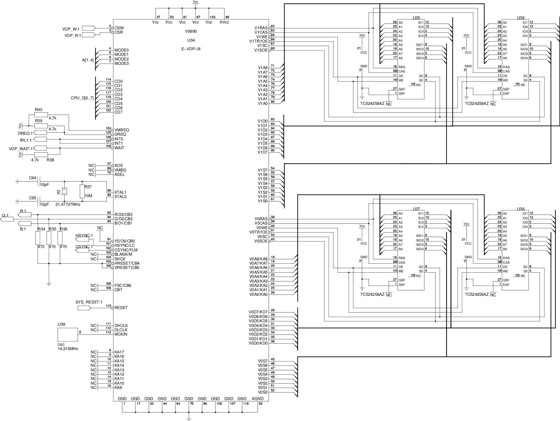
Video circuit (click for full size)
The Video signal is output as RGB only. An CXA2075M RGB encoder is used to convert the video signal into S-Video and composite.
RGB encoder circuit
Despite its commercial flop, it has some nice and advanced features.
- Two pattern screen modes to support tile based games.
- Six different bitmap screen modes. Up to 640x480 display resolution.
- Up to 32768 colors.
- Up to 125 independent sprites in both pattern screen modes.
- Hardware Blitter with drawing functions.
Video circuit (click for full size)
The Video signal is output as RGB only. An CXA2075M RGB encoder is used to convert the video signal into S-Video and composite.
RGB encoder circuit
Audio - Stereo music with two C64 SIDs
The heart of the audio system is the Sound Interface Device (SID)
which is known from the Commodore C64. Kiwi supports two SIDs; one for each channel
to provide stereo audio. The SID has the following features (Wikipedia).

Audio circuit, right channel
The SID has been developed for the C64 which is an 6510 (6502) based computer. 6502 based systems are built around an synchronous bus system. To synchronize with the bus an Phi2 input is provided at pin 6. Phi2 is just the 6502 naming for the E equivalent of Motorola's MC6809 family. So pin 6 is directly connected to the E output of the MC68008.
- three separately programmable independent audio oscillators (8 octave range, approximately 16 - 4000 Hz)
- four different waveforms per audio oscillator (sawtooth, triangle, pulse, noise)
- one multi mode filter featuring low-pass, high-pass and band-pass outputs with 6 dB/oct (bandpass) or 12 dB/octave (lowpass/highpass) rolloff.
- three attack/decay/sustain/release (ADSR) volume controls, one for each audio oscillator.
- three ring modulators.
- oscillator sync for each audio oscillator.
- two 8-bit A/D converters (not used)
- external audio input (audio output of the right channel can be used as input for the left channel by closing a jumper)
- random number/modulation generator
Audio circuit, right channel
The SID has been developed for the C64 which is an 6510 (6502) based computer. 6502 based systems are built around an synchronous bus system. To synchronize with the bus an Phi2 input is provided at pin 6. Phi2 is just the 6502 naming for the E equivalent of Motorola's MC6809 family. So pin 6 is directly connected to the E output of the MC68008.
Floppy disc circuit
Two standard double density floppy disk drives can be used as
mass storage in addition to the harddisk. Almost all neccessery signals are controlled by an Western Digital WD177x
Floppy Disk Controller. But since the WD177x lacks some signals, those have to be controlled by using
some lines of port B of the second PI/T. Port B is shared with the centronics interface.

Floppy circuit part 1, WD177x FDC

Floppy circuit part 2, output driver and termination resistors
To improve signal integrity, almost all signals are actively driven by TTL drivers and terminated by series resistors. There are some minor issues with this circuit. The logic of the drive select and motor signals are not correct in the corresponding picture.
Floppy circuit part 3, PI/T 2 port B
Floppy circuit part 1, WD177x FDC
Floppy circuit part 2, output driver and termination resistors
To improve signal integrity, almost all signals are actively driven by TTL drivers and terminated by series resistors. There are some minor issues with this circuit. The logic of the drive select and motor signals are not correct in the corresponding picture.
Floppy circuit part 3, PI/T 2 port B
8 to 16 bit buffer interface
While the CPU, memory and most of the subsystems are connected with 8 bit width,
there are two subsystems which use a 16 bit bus. These are the ATA/IDE interface and
the Ethernet interface (CS8900a). To access 16 bit with an 8 bit CPU, one has to
break accesses. One 16 bit access works out as two consecutive 8 bit accesses. This works as follows.

8 to 16 bit buffer circuit
To read an 16 bit word, the device is accessed with the first access. While it provides its data, the lower half (D0-D7) is read by the CPU while the upper half (D8-D15) is latched (U44). The second access just enables the output buffer of this latch.
To write an 16 bit word, the device is accessed with the second access. The data provided in the first access is latched (U45). With the next access, the latched data is provided as low byte (D0-D7), while the CPU data is provided as high byte (D8-D15).
As the MC68008 always accesses low byte first, word addressing modes with 16 bit are possible. In this way, the address line A0 can be used to determine the current state of an access. A0 is low for the first and high for the second access.
Parallel ATA/IDE interface
The parallel ATA harddisk interface is mostly an usual 16 bit databus and
a few address and control lines. All electronic (addressable registers) is built into the device.
Hence the name Integrated Device Electronics (IDE). With the usage of the 8 to 16 bit buffer,
most work to provide the PATA/IDE interface has been done. To achieve the correct timing,
an Finite State Machine (FSM) is used. The FSM is part of the CPLD. Finally, to provide signal integrity,
most signals are driven and terminated.

PATA/IDE interface
PATA/IDE interface
Network - 10base-T Ethernet interface
To provide an 10base-T (RJ45) ethernet interface, a crystal logic CS8900a
is used in conjunction with an ethernet transceiver. Although the CS8900a provides an 8 bit mode
it is accessed with 16 bit width since the 8 bit mode does not support interrupts.
As this device has been developed for the Intel bus which is little endian, the databus has
been swapped to connect to the big endian MC68008. Thus the data lines D0-D7 coming from the 8 to 16
bit buffer are connected to data lines SD8-SD15 of the CS8900a and vice versa.
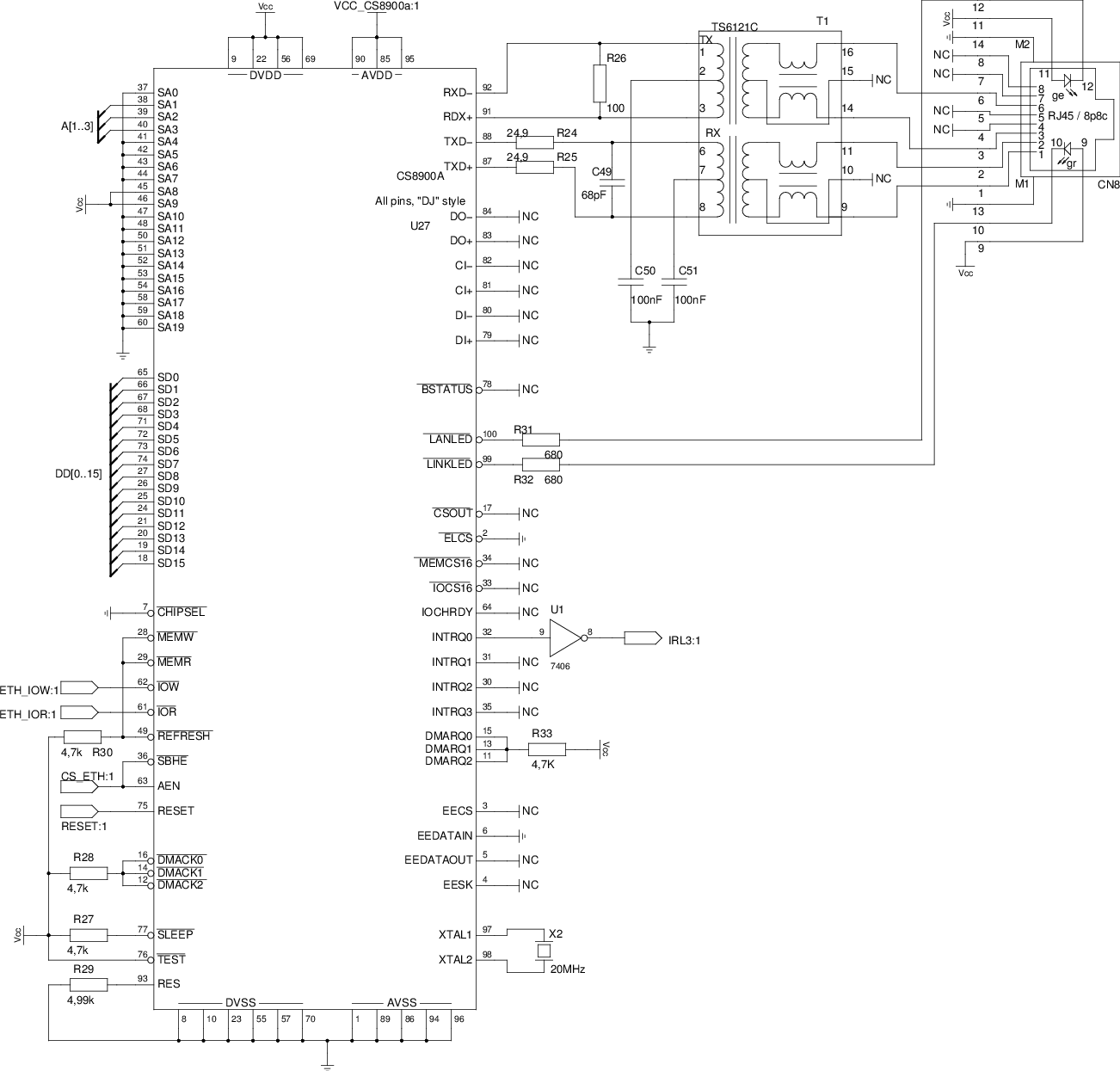
Ethernet interface with CS8900a (click for full size)
Ethernet interface with CS8900a (click for full size)
Time and date - real time clock
The real time clock (RTC) is battery backed up, but unfortunately, the design is not
clean enough. The datasheet claims an voltage monitor to prevent accesses by accident
when the computer is switched on or off. The voltage monitor was replaced by just two
diodes (D1 and D2). These prevent current flow from the battery into the system when
switched off and charging the battery when switched on.
Sometimes switching off and on changes parts of the time and date.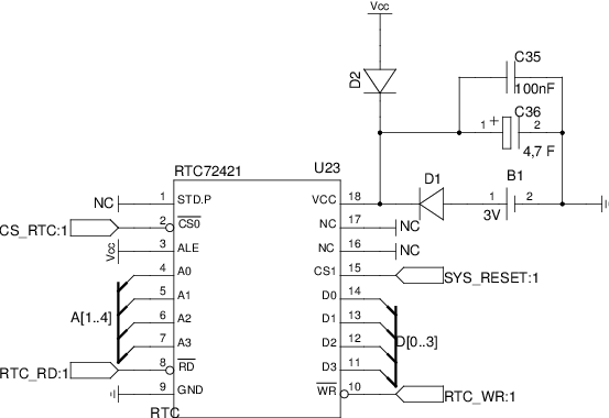
Real time clock
Sometimes switching off and on changes parts of the time and date.
Real time clock
Interrupts
As mentioned in the chapter about the CPU, the MC68008 supports different
interrupt level. The level is encoded with three pins *IPL0-IPL2.
Interrupt level
The MC68008 supports two types of determining the interrupt vector. Autovector and non autovector
interrupts. By implementing non autovector interrupts, the interrupting device provides its own
interrupt vector within an acknowledge cycle. Kiwi uses the autovector mode. This mode hard ties
every interrupt level to exact one vector. If an interrupt level is shared, the source has to be
determined within the service routine.
| *IPL2 | *IPL1 | *IPL0 | Interrupt level | used by |
| 1 | 1 | 1 | 0 | no interrupt |
| 1 | 1 | 0 | 1 | V9990 |
| 1 | 0 | 1 | 2 | IDE |
| 1 | 0 | 0 | 3 | CS8900a |
| 0 | 1 | 1 | 4 | WD177x |
| 0 | 1 | 0 | 5 | PI/T 2, timer |
| 0 | 0 | 1 | 6 | DUART |
| 0 | 0 | 0 | 7 | not used |
Glue logic - how everything is tied
A Xilinx XC95108 CPLD is used to avoid a lot TTL logic. The built in
functions are divided into following groups.
- address decoder
- FSM (finite state machine) for DRAM access and refresh
- FSM for accessing the V9990
- FSM for PATA/IDE timing
- FSM for buffer interface timing
- *WR and *RD strobe generator
- clock divider to generate CPU clock
...
        setstate : process(CLK, RESET)
        begin
        if (CLK = '1' and CLK'event) then
          if RESET='0'
                then STATE <= IDLE;
                else STATE <= NEXTSTATE;
          end if;
        end if;
        end process setstate;
...
        getnextstate : process(CLK, STATE, REFREQ, MEMREQ, RW_SYN, AS, DS,
                               AS_SYN, DS_SYN)
        begin
        case STATE is
          when IDLE => if (REFREQ = '0')
                         then NEXTSTATE <= REFRESH2;
                       elsif (REFREQ = '1' and MEMREQ = '0')
                         then NEXTSTATE <= MEM1;
                       else NEXTSTATE <= IDLE;
                       end if;
          when MEM1 => NEXTSTATE <= MEM2;
...